

VHX-7000 digital microscope examines semiconductor quality
The trend to miniaturise components to satisfy the ever-increasing demand for wearable and mobile devices has enabled a myriad of tiny yet functionality-packed ICs to be inserted onto a single PCB. However, one of the issues of working in these miniscule sizes has been the difficulty of research and development professionals checking prior to mass production whether on-board components meet the stringent quality requirements that ensure they will operate reliably and repetitively throughout the life of the device.
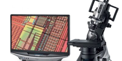
Claiming to transform the way that R&D inspection work is carried out on semiconductors, Keyence has introduced what it says is the world´s first 4K ultra-high accuracy microscope. The VHX-7000 digital microscope can inspect samples and deliver greater convenience to view, capture and measure. This means its images can rival those of scanning electrode microscopy (SEM) – especially when the optical shadow effect mode feature is enabled, it says..
The VHX-7000 delivers the highest definition in the history of microscopes, says Keyence, and offers a depth-of-field 20 times higher than conventional optical microscopes. It also has a simple user interface, sub-menus and step-by-step guide for ease of use – even a novice could capture the highest resolution IC images, boasts Keyence.
Another key feature is the 1Tbyte hard drive that is also integral to the microscope (which is based around a Windows 10 PC). This enables images to be saved on the device and shared over a network or via a USB drive. Detailed reports can also be produced automatically in Excel format for instant sharing with colleagues.
The all-in-one VHX-7000 obviates the need to buy several different microscopes and is highly cost-effective when compared to an SEM. It can be upgraded and customised and is available with different stages, stands and optional features such as the motorisation of axes and a range of optical lenses that can be added to the base model.
The 4K VHX-7000 is particularly suited to the semiconductor market and surpasses traditional lens-based microscopes that rely on eyepieces. As well as its superior magnification of minute features (from 20x to 6000x), it has the ability to subtly shift the finely-tuned XY motorised stage automatically to increase resolution by 33 per cent. The ´stitching´ of several individual images function has been simplified due to the powerful on-board software with intelligent algorithms that are capable of evening out lighting and diffusing it over the inspected part.