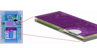
Nanusens shrinks sensor and control circuit for ASICs with embedded sensors
By simultaneously shrinking the sensor and control circuit, Nanusens has created a digital circuit design to measure the capacitance of its nanosensors to create ASICs with integrated sensors. Both the sensor structure and its detection circuitry can be made at the same time within a chip using standard CMOS processes on whatever process node is required, explained the company. As a result, ASICs can now be made with several sensors embedded within them. Integrating sensors as IP blocks offers dramatic reductions in costs and size, claimed Nanusens, as it completely replaces the current solution of discrete sensor packages.
“This is a major milestone for the company,” said Dr. Josep Montanyà, CEO of Nanusens. “The first was successfully making our unique, nanoscale, sensor structures within the CMOS layers. This solves the problem that conventional MEMS have to be made on custom production lines that have limited production capabilities whereas we can make almost unlimited numbers of our sensors in CMOS fabs. These are available in standard packages such as LGA, QFN, WLCSP and others, but, like all other MEMS sensors, they require analogue circuitry to detect tiny capacitance changes coming from nano-displacements of their devices in operation. Our breakthrough is the creation of a fully digital detection circuit as this can be scaled down to the process node being used for the sensor structure and pairs to form a complete sensor and detection solution.
Shrinking the sensor and circuitry simultaneously enables the company to take advantage of smaller CMOS geometries which include reduced costs and reduced power consumption of more than 10 times compared to analogue detection circuits. “This is impossible for other MEMS sensor solutions as their structures cannot be shrunk neither can their analogue circuits as their transistors need a large area to maintain the required low levels of noise,” said Montanyà.
The all-digital detection circuit provides a very fast on / off switching of the circuit of three microseconds compared to 300 microseconds or several milliseconds in conventional analogue transconductance / charge amplifier or similar circuits, said Nanusens. This is advantageous for applications which require a low sampling frequency, such as motion detector applications where the motion detector is typically used to wake up the rest of the device. If the device is in sleep mode most of the time, the battery life is dependent on the current consumption of the motion detector. The fast on / off of the new digital detection circuit results in sub micro A current consumption on the 180nm test chip, which more than doubles the battery life in these applications.
“Instead of being discrete packages on a PCB or a multi-die solution, all the required sensors can be integrated into an ASIC just like another IP block,” said Montanyà. Portable multi-sensor devices, such as smart phones, ear buds and smart watches will benefit from the reduction in BoM, size and power budget and Nanusens confirmed that it is in discussion with companies who want to license this IP.
Founded in 2014, Nanusens is headquartered in Paignton, Devon, England with R & D offices in Barcelona, Spain and Shenzen, China.


