

Medical implants get onboard with PCB growth
The global PCB market is expected to grow at 3.44 per cent CAGR between 2017 and 2015, driven by many factors, not least the IoT and medical devices, where implants are creating interest in miniature PCBs, writes Caroline Hayes
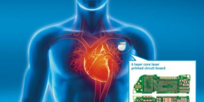
Miniature PCBs are used in medical devices such as medical treatment, monitoring of blood sugar, blood pressure, and for diagnosis or imaging applications, such as x-ray and ultrasound. They are also used in pacemakers, defibrillators, hearing aids, with intelligent adjustment, local neuro-simulators for pain therapy and cochlear implants.
Figure 1: AT&S supplies PCBs for medical therapy devices, such as pacemakers and defibrillators
Treatment and monitoring are both made easier with miniature, implantable medical devices. The global medical electronics market is expected to reach $4.4 billion by 2022, a growth of over five per cent, per annum in that period. The realisation of creating, and validating, miniature PCBs for use in medical devices is not just a case of making the circuits smaller, they also need to formed differently and certified to international standards for medical devices. These include the IEC 60601-1, for electrical equipment transferring energy to or from the patient and the ISO 10993.
Other challenges are the identification and selection of biocompatible materials and digitisation to ensure data is collected and transmitted.
“Medical technology is facing great challenges with regard to demographic changes and the modern lifestyle,” says Walter Moser, chief sales officer of the automotive, industrial and medical business unit at Austrian PCB supplier, AT&S.
He goes on to explain that the company works with customers to find solutions: “That includes new cost-efficient, patient-friendly treatments and diagnostic procedures, as well as user-optimised monitoring solutions,” he says.
The company portfolio consists of double sided and multi-layer PCBs, flexible and rigid PCBs, insulated metal substrate and IC substrates. AT&S says it is one of only a few PCB manufacturers certified to EN ISO 13485, the standard for medical devices
Cleaning procedures
Mike Jones, vice president, international sales, for MicroCare, points out that the increase in complex, miniature components, and ever-tight tolerances cause their own problems that may be unfamiliar to consumer electronics manufacturers.

Figure 2: Whatever the shape, PCBs for medical devices must be effectively cleaned before processing (Picture – AT&S)
Medical devices have to be tested for safety, quality and predictability, rather than pass muster as ‘good enough’ as is the case with consumer electronics. Microcare, specialises in cleaning electronics during manufacture, rework and repair and advocates post-assembly cleaning of PCBs and mechanical assemblies to minimise production and performance issues, especially as the PCBs become smaller and more densely populated.
The company is looking at variations and ‘tweaks’ to the vapour degreasing process, for example, to optimise cleaning, throughput or costs. As the processing functionality increases, companies are looking at the fluxes used in densely populated, miniature PCBs. Cleaning can influence the active fluxes that are used, which affect the quality of solder joints. Other concerns are cold joints, insufficient wetting, bridging and shorts, all of which adversely impact performance. Delay in testing for medical approval can be costly in the competitive medical market.
To remove fluxes, as well as adhesives, conformal coatings, fingerprint residue and other contaminants from the PCB, the conventional option of aqueous cleaning is being replaced with solvent cleaning, as the medical PCBs evolved into smaller, often intricately shaped, parts, for which solvent cleaning was consistent, quick and more cost-effective.
Microcare is re-energising vapour degreasing with some adaptions to meet environmental issues as well as medical manufacturing standards. For example, using solvents that boil at 40 degree C, means less electricity is used. They also have a lower surface tension and lower viscosity than water to clean under extremely small parts, yet are dense enough to dislodge particulate from components, whatever the shape.
Using vapour degreasing, the parts are dry and immediately available for processing.
Solvents are inimical to bacteria, so solvent cleaning ensures a pyrogen-free cleaning environment, whereas bacteria grows in water.