

Editors Blog – The benefits of miniaturisation make for a comfortable fit
Some interesting development work is being done to make sure that sensors and antennae are fit for purpose in wearable devices, writes Caroline Hayes
Breakthroughs in antenna technology will reduce the size of wearable devices without adversely impacting performance. One was shown at MWC Americas, where Altair Semiconductor and Ethertronics, a subsidiary of AVX, showcased an antenna prototype that is expected to enable small end-products.
The prototype uses Ethertronics’ small antenna with Altair’s ALT1250 dual-mode Cat-M1/NB-IoT (narrowband IoT) chipset algorithms.
The ALT1250 is an LTE release 13 CAT-M1 and NB1 IoT chipset (Figure 1) with low power consumption, which is important for battery-operated devices used in the IoT or with wearable devices. OneSKUTM RF technology enables multiple LTE band combinations in a single hardware design.

Figure 1: Altair Semiconductor’s ALT1250 is an integrated LTE CAT-MI and NB IoT chipset
It integrates an LTE baseband processor, a radio frequency integrated circuit (RFIC), a power management unit (PMU), memory, power amplifiers, filters and antenna switch, as well as a global navigation satellite system (GNSS), a cellular based location engine and microcontroller subsystem. Even with external components, the size of modules based on the ALT1250 is less than 100mm2.
To extend battery life to over 10 years, there is a variety of power modes, including 3GPP PSM and eDRX.
Combining Altair’s algorithmic capabilities with Ethertronics’ expertise in the design of antenna and tunable components, resulted in the smallest antenna design for cellular, wearable devices and other small form factor IoT devices, says Dima Feldman, head of product management for Altair. He continued that the combination is “setting a new standard for antenna performance that improves coverage, power efficiency and overall user experience”.
Sensor capacity
Another company, Nanusens, has applied innovative technology to reduce the size of sensors to reduce the form factor or to make room in products for other functionality or a battery.

Figure 2: Nausens’ nanotechnology saves volume and PCB estate
The company specialises in nano sensors which are integrated into a CMOS chip and claims that its technology increases battery life of earbuds by up to 20 per cent by replacing MEMS sensors in an earbud with a single multi-sensor chip that is up to 10 times smaller than alternatives currently available, to make room for larger batteries.
Using nanoscale technology, the company produces the sensors within the CMOS chip that also integrates the control circuitry. Conventional sensor packages consist of two chips, one with the MEMS sensor and one with the control electronics. Nanusens claims that its Nano Electro Mechanical Systems (NEMS) package at 1.0mm3 reduces volume by 3.0mm3.
The Inter Metal Dielectric (IMD) is etched away through the pad openings in the passivation layer using vapour HF (vHF) to create the nano sensor structures. The holes are sealed and the chip packaged. Standard CMOS processes with minimal post-processing are used and the sensors can be directly integrated with active circuitry as required. The company reports that the sensors can potentially have high yields similar to CMOS devices and that production is fab-independent.
The company concedes that although more space can be saved the more MEMS packages are replaced, the size of the Nanusens chip increases slightly with every additional sensor function. The PCB estate saved using the integrated sensor package can be used to increase the size of the battery or add a supercapacitor to extend the battery life in wearable devices such as earbuds.
Dr Josep Montanyà, CEO Nanusens, explains “While some manufacturers want more battery life by using a larger battery or a supercapacitor, others want to use some of this freed-up space for features such as memory so that songs can be stored locally on the earbud. This is another way to extend the battery life as songs would not need to streamed over Bluetooth, again giving longer audio on the go.”
The NEMS design is more robust than MEMS designs, says the company, as it is less affected by problems of stiction caused Van der Waals or Casimir forces. that create reliability issues for MEMS. Please see Nanusens release on stiction at:

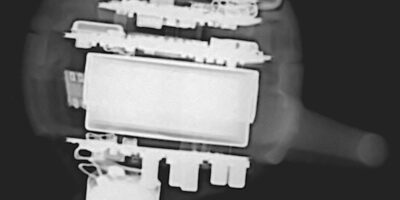
Figure 3: An x-ray of earbuds using a NEMS sensor showing battery and electronics
At MWC19, in Barcelona, Spain this month, Nanusens will introduce its nano sensor technology (stand 6M14).
The adaptable technology can be used to create a range of sensors. A 2D motion detector for earbuds is scheduled for release Q4 2019. It can be used to implement tap and double tap for control, wake-on-movement and sleep-on-rest functions. Following that, a 3D accelerometer and a bone conduction sensor for noise cancellation, will each be integrated in the single chip.
Chips will be available in a small package, such as WLCSP, or as bare die that can be attached directly to the PCB.