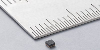
PowerHap development starter kit provides design feedback

A development starter kit for fast haptics prototyping gives mechanical designers and engineers a first impression of haptic feedback with PowerHap piezo actuators. The kit by TDK shows how the mechanical integration works, and provides a reference design, which can be adapted to various applications.
TDK’s PowerHap piezo actuators offer haptic feedback based on acceleration, force, and response time. They can be used in automotive designs (e.g., steering wheels, displays, dashboards, buttons), smartphones, displays and tablets, household appliances, ATMs and vending machines, game controllers, VR gloves, industrial equipment and medical devices.
The PowerHap Starter Kit (ordering code: Z63000Z2910Z01Z73) consists of a seamless button assembly (including PowerHap 1204H018V060 and PowerHap 1313H018V120), a round button assembly (incling PowerHap 1204H018V060), the BOS1901-Kit driver board from Boréas Technologies, additional PowerHap devices (including an FPC connection cable), USB cable, and a quick start user guide.
The BOS1901-Kit platform in the starter kit is pre-programmed for the seamless button and the round button for an immediate experience of sensing and haptics with the PowerHap actuators. The features of the Boréas platform make it easy to customise and tailor the haptic experience by adjusting the sensing detection parameters and the haptic feedback waveform.
TDK is based in Tokyo, Japan. It was established in 1935 to commercialise ferrite, a key material in electronic and magnetic products. Today, TDK‘s portfolio features passive components such as ceramic, aluminium electrolytic and film capacitors, as well as magnetics, high-frequency, and piezo and protection devices. The product spectrum also includes sensors and sensor systems such as temperature and pressure, magnetic, and MEMS sensors. In addition, TDK provides power supplies, energy devices and magnetic heads. Products are marketed under the product brands TDK, Epcos, InvenSense, Micronas, Tronics and TDK-Lambda.
TDK focuses on demanding markets in automotive, industrial and consumer electronics, and information and communication technology. The company has a network of design and manufacturing locations and sales offices in Asia, Europe, and in North and South America.

> Read More

ams Osram lights up TriLite’s laser beam scanner for smart glasses

RGB laser diodes by ams Osram will illuminate TriLite’s Trixel 3 laser beam scanner in a collaboration whereby the compact, lightweight scanner will enable augmented reality for smart glasses and other consumer applications. 

> Read More

Smiths Interconnect describes Kepler as breakthrough contact technology  

Two axis motion during a single actuation of the test socket is provided by the Kepler contact technology. It has been developed by Smiths Interconnect, and is claimed to the only contact technology for IC testing to provide this will boosts first pass yield. It is also claimed to enhance production reliability and extend maintenance intervals.
The technology can be used for testing high performance computing, wearables or automotive chips, confirmed Smiths Interconnect.
Presently, the semiconductor test industry uses the traditional vertical spring probes for BGA, LGA, QFN, and QFP packaging testing, or cantilever scrubbing contact design has been used in peripheral segments to remove surface oxides and contaminants. Both technologies, however, require maintenance and performance monitoring to ensure optimal results during testing cycles.

> Read More

MRigidCSP package is claimed to increase MOSFET’s mechanical strength  

Robust package technology, MRigidCSP, by Alpha and Omega Semiconductor (AOS), is initially offered on its AOCR33105E, 12V, common drain, dual N-channel MOSFET. The packaging technology is designed to decrease on resistance while increasing mechanical strength, and is particularly suited to battery applications in smartphones, tablets and ultra-thin notebooks.
AOS explained that fast charging, which requires lower power loss in the battery management circuit, is now widely adopted for portable devices. As the charging currents increase, ultra-low electrical resistance is needed for improved performance. In standard wafer-level chip scale packages (WL-CSPs), the substrate can be a significant portion of the total resistance when back-to-back MOSFETs are employed in battery management applications.  A thinner substrate reduces the overall resistance but drastically reduces the package’s mechanical strength. This reduction of mechanical strength can lead to more stress during the PCB assembly reflow process, potentially causing warping or cracking in the die and, ultimately, failure in the application. The AOCR33105E is designed with trench-power MOSFET technology in a common drain configuration for design simplicity. It features low on resistance with ESD protection to improve performance and safety in battery management, such as protection switches and mobile battery charging and discharging circuits.
“Incorporating the AOS MRigidCSP packaging technology with our new dual N-channel MOSFET combines electrical performance improvements with the benefit of high robustness,” said Peter H. Wilson, senior MOSFET product line marketing director at AOS.
AOS designed the MRigidCSP package technology to be used with high aspect ratio CSP die sizes. The CSP construction delivers “a significantly strengthened battery MOSFET that won’t warp or break during the board manufacturing process,” added Wilson.
The AOCR33105E is available in a 2.08 x 1.45mm package, with RDS(on) of 3mOhm at 4.5V / 4.2mOhm at 3.1V.
The AOCR33105E in the MRigidCSP package is immediately available in production quantities with a lead time of 14 to 16 weeks. It is RoHS 2.0 compliant and is halogen-free.

> Read More

About Weartech

This news story is brought to you by weartechdesign.com, the specialist site dedicated to delivering information about what’s new in the wearable electronics industry, with daily news updates, new products and industry news. To stay up-to-date, register to receive our weekly newsletters and keep yourself informed on the latest technology news and new products from around the globe. Simply click this link to register here: weartechdesign.com