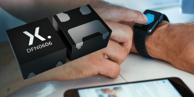
MOSFETs for wearables are 36 per cent smaller says Nexperia
MOSFETs in the DFN0606 package for mobile and portable applications have been released by Nexperia. They are claimed to be 36 per cent smaller compared to previous-generation DFN1006 parts. They also have the lowest RDS(on) for their size, says the company.
The MOSFETs employ the commonly used pitch of 0.35 mm to simplify PCB assembly processes. The PMH family of MOSFETs have a footprint of just 0.62 x 0.62mm. According to Nexperia, advanced process technology means the new devices offer the lowest RDS(on) in the market, with more than 60% reduction compared to competitor devices. Coupled with the MOSFETs’ ESD performance, and VGS low voltage threshold down to 0.7V, the MOSFETs are particularly suitable for for portable applications with low drive voltage.
Nine PMH devices in the new DFN0606 package are available now.
Nexperia provides essential semiconductors, components that are required by every electronic design in the world. The company’s extensive portfolio includes diodes, bipolar transistors, ESD protection devices, MOSFETs, GaN FETs and analogue and logic ICs.
The company is headquartered in Nijmegen, Netherlands. Nexperia annually ships more than 90 billion products, each meeting the stringent standards set by the automotive industry. These products are recognised as benchmarks in efficiency – in process, size, power and performance — with industry-leading small packages that save valuable energy and space, says Nexperia.


