

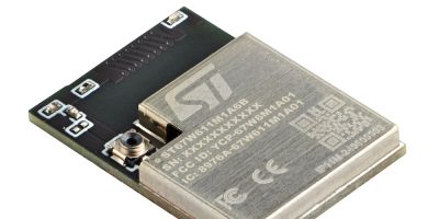
ST has introduced the first product of its strategic collaboration with Qualcomm Technologies to simplify development of next-generation wireless solutions for industrial and consumer IoT applications. The collaboration aims to deliver initially IoT modules leveraging ST’s powerful STM32 ecosystem and Qualcomm Technologies’ leading wireless connectivity solutions.
IoT
Rutronik introduces the new SoCs from Nordic Semi for next-generation (I)IoT applications
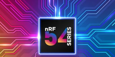
With three SoCs from the new nRF54L series, the nRF54L15, nRF54L10 as well as nRF54L05, Rutronik is expanding its portfolio of Bluetooth Low Energy Systems-on-Chip (SoCs) from Nordic Semiconductor. Higher performance, efficiency and security make this recently launched product the optimal and future-proof choice for realising the next generation of wireless IoT products.
Microchip releases 20 Wi-Fi products for industrial and commercial applications

With Industry 4.0, the rapid rise of Artificial Intelligence (AI), digitised manufacturing and the age of IoT everything, the demand for wireless connectivity in commercial and industrial applications is growing at an exceptional pace. These applications typically require reliable connectivity that can withstand extreme environments that are exposed to high temperatures, background noise and obstructions. To help meet this need, Microchip Technology has added 20 products to its Wi-Fi® portfolio.
ST reveals Page EEPROM two-in-one memory to boost smart-edge performance and efficiency

ST’ Page EEPROM combines the power efficiency and durability of an EEPROM with the capacity and speed of a Flash memory, creating a hybrid memory for applications that face extreme size and power constraints.
About Weartech
This news story is brought to you by weartechdesign.com, the specialist site dedicated to delivering information about what’s new in the wearable electronics industry, with daily news updates, new products and industry news. To stay up-to-date, register to receive our weekly newsletters and keep yourself informed on the latest technology news and new products from around the globe. Simply click this link to register here: weartechdesign.com