

Miniaturised PCBs have designs on wearable medical devices
As systems and components for therapy, diagnosis and patient monitoring are getting smaller, but more powerful, safety and reliability are a priority in electronic design. AT&S believes it is one of the few PCB manufacturers that is certified to EN ISO 13485, the standard for medical devices.
The miniaturisation of medical assemblies requires extremely small interconnection and very small PCB dimensions, bringing challenges. For example, conductor track widths and distances are currently only 50 micron and are getting smaller. Electrical connections of the individual layers are realised using minute stacked vias and the solder resist has to be positioned precisely. The use of modern manufacturing techniques and materials are essential to be able to meet all these exacting requirements in the production process in a reproducible and reliable manner, says AT&S.
The company supplies PCBs for hearing aids. For modern cochlear designs, flexible PCBs with two to six layers are required. Due to the small installation space, the miniature systems are designed as high density interconnection (HDI) or stacked via circuits.
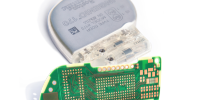
Implantable heart rhythm, pacemakers or defibrillators use PCBs that have special regulations for process control, which are specified and described in international standards. Materials used must also satisfy specific criteria, which are regularly checked in extensive qualification tests.
HDI circuits are also used for the control and adjusting unit of prostheses. Flexible PCBs are used in the prostheses to implement the dynamic movement. To accommodate the constant movement and small bending radii, a flexible base material with rolled copper is used to ensure the required bending cycles and the low bending radii.
Compact interconnection for wearables and tracking systems for patient monitoring and medical lifestyle applications range from mobile medical measuring devices for blood pressure measurement to smart watches and fitness trackers. Here, 2.5D technology offers advantages for the implementation of cavities. The defined indents (cavities) in the PCBs can be used to lower electronic components, such as sensors and even logic components, to reduce the thickness of the PCB.
http://www.ats.net